One integrated
Sion hardware
stack.
Each pillar is world-class on its own. Their real power comes from working together under one accountable program — chip to board to system, owned end-to-end by Sion.
SILICON IP &
INTEGRATION
NRZ & PAM4 SERDES
Production-proven high-speed SerDes across 7nm, 5nm, 3nm
Gen5 / Gen6 · CXL 3.0
Root complex, endpoint, switch, and fabric controllers
400G / 800G MAC & PHY
MAC, PCS, FEC, with optional TSN support
HBM3e / DDR5 / LPDDR5X
Controllers, PHY, and memory fabric
AI-optimized NoC
Coherent and non-coherent fabric for AI SoCs
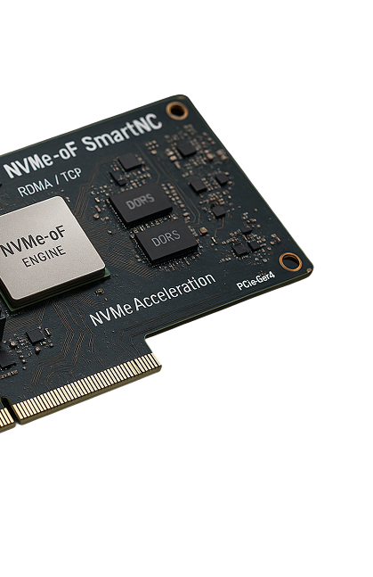
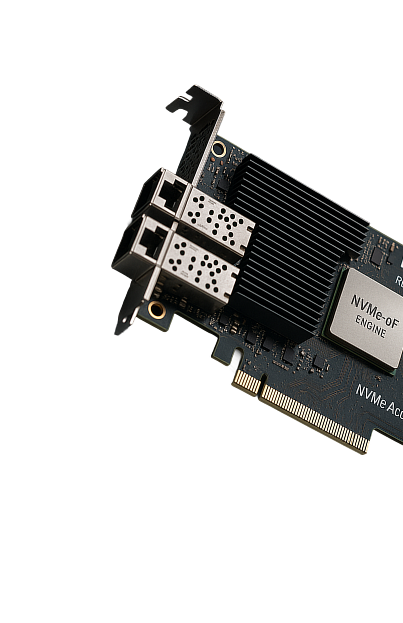
NAND ECC & NVMe
ECC engines, NAND interface, computational storage IP

CHIP & SOC
DESIGN
RTL & Architecture
Micro-architecture, RTL coding, low-power design, clock & reset architecture
UVM · Formal · Emulation
SystemVerilog/UVM, formal, coverage closure, Palladium/Protium emulation
7nm / 5nm / 3nm PD
Floorplan, P&R, timing/power closure, signoff at advanced nodes
Design for Test
Scan, MBIST, LBIST, boundary scan, high-speed ATPG closure
Bring-up & Validation
Lab bring-up, SerDes tuning, compliance, characterization
Ramp to Volume
Test program development, yield enhancement, supply-chain partnering
Hardware Systems &
Platforms
PCIe / CXL / 800G
Signal integrity, impedance control, thermal management
Deployable AI Systems
Full-rack AI accelerator platforms ready for hyperscaler deployment
Embedded & RTOS
SoC firmware, device drivers, bootloaders, secure boot
Validation & Testing
PCIe-SIG, CXL Consortium, OCP, UCIe test readiness
Chassis · OCP Racks · BMC · Data-Center-Ready Platforms
Sion extends hardware delivery beyond the card — engineering the full system around it. 1U / 2U / 4U chassis design, OCP & 19″ rack integration, backplane & midplane design, rack-level signal integrity & thermal budgeting, BMC firmware, power sequencing, and cable management. The layer that turns a working card into a deployable, rack-ready platform for AI, storage, and networking customers.
Three ways to engage Sion.
One team that delivers.
From pre-packaged hardware offerings with same-day quotes to full multi-year strategic partnerships — Sion structures engagements to match your risk, timeline, and commitment profile.
 PRODUCTIZED OFFERING
Pre-scoped, pre-priced engagements with clear deliverables. From SilicaBoost™ IP integration to StorageCore™ turnkey controllers — start engineering in weeks, not months.
Dedicated TeamA ring-fenced Sion engineering team embedded with your program, scaling up and down with your roadmap. Ideal for verification, PD, board design, firmware, or multi-project capacity.
Strategic PartnershipA multi-year, multi-program partnership with shared investment, co-developed IP, and deep executive alignment. Reserved for customers with a long-term hardware roadmap.

A proven path from
concept to production-
ready hardware.
ARCHITECTURE &
FEASIBILITY
Joint architecture review, IP selection, node selection, power/performance/area estimation, and program-risk assessment.
RTL DESIGN &
VERIFICATION
Micro-architecture, RTL coding, UVM/ SystemVerilog testbench, formal property verification, coverage closure, and optional emulation on Palladium/Protium.
PHYSICAL DESIGN &
SIGNOFF
Floorplan, placement, CTS, routing, timing closure, power signoff, DRC/LVS, EM/IR closure — all at advanced nodes with full vendor-flow support.
TAPE-OUT & SILICON
BRING-UP
Foundry interface, mask prep, wafer fabrication monitoring, package design, lab bring-up, SerDes tuning, compliance testing, characterization.
BOARD, FIRMWARE &
SYSTEM INTEGRATION
High-density board design, firmware development, device drivers, reference platform integration, and system-level bring-up — turning Sion silicon into a shippable hardware product.
NPI & PRODUCTION
RAMP
Test program development, ATE program optimization, yield enhancement, supply-chain partnering, and ramp to volume — delivering a production-ready hardware solution.
Your IP is protected.
Your program is
compliant.
We know IP leakage is the single biggest concern for AI and defense-adjacent customers. Sion operates with enterprise-grade process controls, segregated project environments, and clear Chinese-wall protocols on every engagement.
Export-control awareness, ITAR-sensitive handling procedures, and audit-ready data-room practices are built into every Sion engagement — not bolted on.
Information Security
Export Compliance
Project Isolation
Multi-tier IP Controls
Let's scope your
hardware program together.
A 30-minute architecture call with a Sion solution architect is the fastest path to a scoped proposal — for a chip, a board, a full system, or all three.