
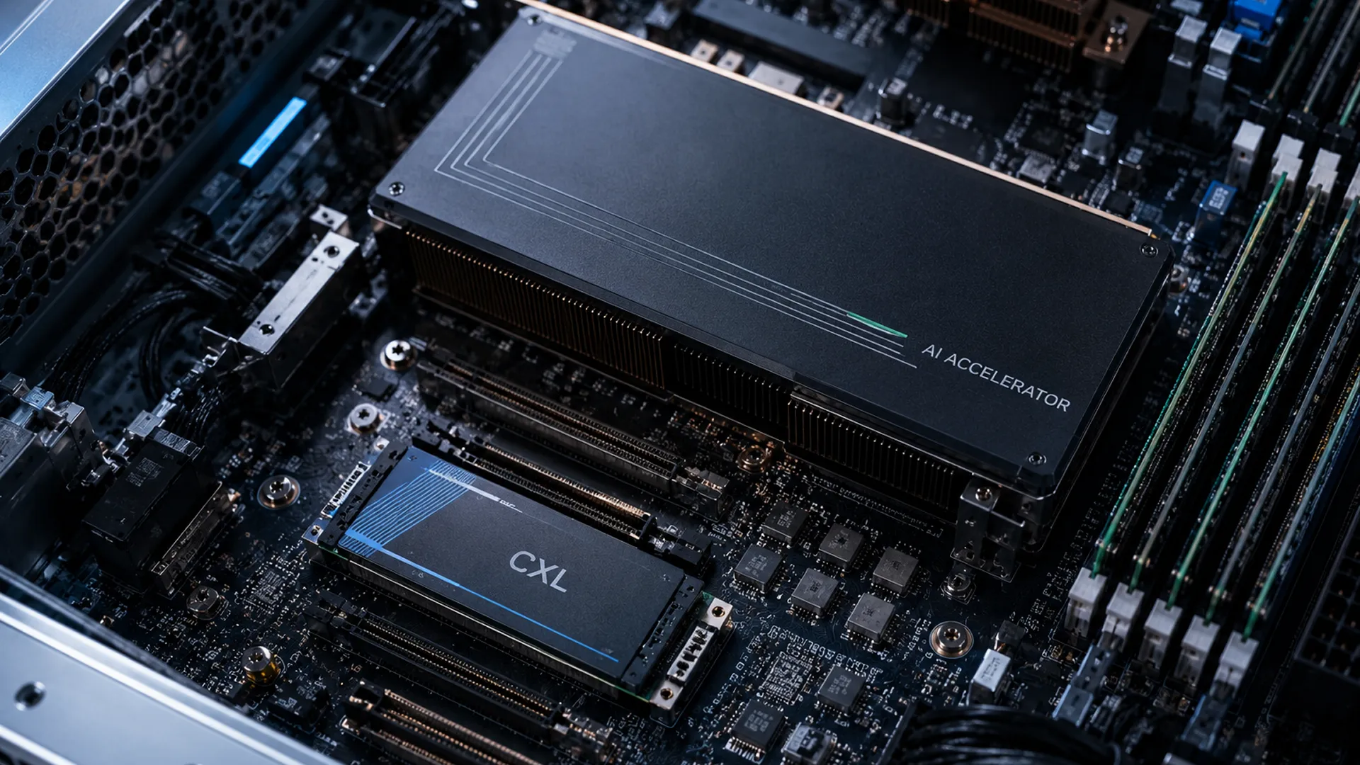
Custom 7nm AI accelerator card with HBM3 and CXL 2.0 — first silicon in under 14 months.
Hyperscaler-Track AI Startup
· Series C · Bay Area
14 months (Architecture
→ First Silicon) ·
22 months to GA card
SoC architecture · RTL
· Verification · PD · Tape-out ·
PCIe card · Firmware · Drivers
42 engineers across Bangalore,
San Jose & Singapore
 THE CHALLENGE
Beat the hyperscaler evaluation window.
A well-funded AI startup had a differentiated model-serving IP in FPGA form — but their hyperscaler customer had opened a 24-month evaluation window for custom accelerator cards. To be in the race, the startup needed a production ASIC, a PCIe Gen5 accelerator card, firmware, and a driver stack — all within that window. A missed window meant a missed multi-hundred-million-dollar opportunity.
WHY SION WAS CHOSEN The only partner offering chip + card + firmware under one SOW.
The customer was a 90-engineer startup — exceptional at ML architecture, but with no in-house silicon, board, or firmware experience. They needed a partner who could own the entire hardware delivery path while they focused on ML IP. Sion's 24+ prior tape-outs at 7nm and proven high-speed SerDes and HBM3 integration expertise made the shortlist a formality.
7nm
Advanced-node execution

24+
Prior production tape-outs
What Sion Delivered —
End-to-End
From customer RTL to deployable card.
SoC Architecture & Integration
Full SoC architecture around the customer's ML compute IP, NoC fabric design, CXL 2.0 subsystem, HBM3 memory controller integration, and host-PCIe Gen5 subsystem.
RTL Integration & Verification
SoC-level integration, full UVM verification environment with 95%+ functional coverage, formal property verification on PCIe/CXL controllers, and gate-level signoff.
Physical Design & 7nm Tape-out
Full-chip 7nm physical design, high-speed SerDes integration, HBM3 PHY signoff, power-grid design for 350W, DFT insertion, and successful first-silicon tape-out.
Accelerator Card Design
OCP-compliant PCIe Gen5 x16 card with HBM3 integration, thermal solution for 350W air-cooling, power delivery for 8×48V rails, and manufacturability review.
Firmware, Drivers & BSP
Card-side firmware, Linux host drivers, DMA engines, customer-runtime integration plugins, and platform BSP for the target hyperscaler reference server.
Bring-up & Customer-Site Deployment
Lab bring-up, performance tuning, customer-site validation, co-deployment with the customer into the target hyperscaler reference environment, and issue resolution to GA.
First silicon on schedule. Into the customer's hyperscaler evaluation with weeks to spare.
14 mo
To first siliconArchitecture kickoff to working chip in hand
100%
First-silicon successNo respin required — PCIe, CXL, HBM3 all functional
3 WKS
Lab bring-up to customer sampleFrom first power-on to customer-site deployment
Series D
Customer ClosedOn the back of a working, production-grade product
Why This
Mattered
— THE SION difference
Advanced-node execution discipline, not promises.
For an AI startup racing a hyperscaler evaluation window, "first silicon" is everything — it is the difference between a multi-hundred-million-dollar contract and a down round. Sion's ability to own every layer from SoC architecture through firmware drivers meant the customer's 90-person team could stay focused on ML differentiation while Sion carried the hardware execution. First silicon worked on the first try — a rare feat at 7nm with HBM3 and advanced CXL integration.
Real programs.
Verifiable references.
Customer identities are held confidential under mutual NDA. Technical scopes, outcomes, and program structures shown on this page are representative of actual Sion engagements across storage, AI infrastructure, and networking. Full technical deep-dives, architecture reviews, and direct reference calls are available to qualified prospects under mutual NDA.

24+
PRODUCTION TAPE-OUTS
3nm
ADVANCED-NODE EXPERIENCE
Top 5
SEMI CUSTOMERS SINCE 2021
ISO
GRADE IP-PROTECTION PROTOCOLS
Your program. One accountable team.
Start the scoping call.
Under mutual NDA, we walk you through full technical deep-dives of the programs shown above, connect you with customer references, and map your hardware challenge to a Sion engagement model.